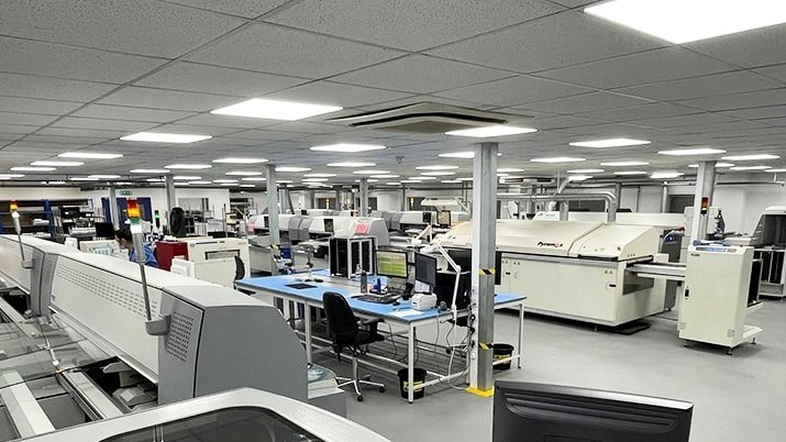
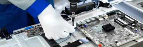
Electronics Manufacturing Services
As high-performance technology continues to evolve, it’s becoming smarter, more compact and lighter than ever before. These qualities are crucial for keeping your products at the forefront of innovation, allowing them to maintain a competitive edge in the market. With precision and consistency as our focus, TechPoint supports clients with professional PCB production from initial concepts through to volume manufacturing. Our skilled team and state-of-the-art production facilities, paired with comprehensive technical and consultation services, mean we can bring your ideas to life with efficiency and confidence. Find out more about our EMS services below:
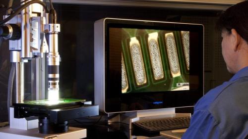
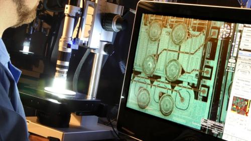
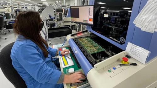
3D Automatic Optical Inspection (AOI) & 3D Automatic X-ray Inspection (AXI)

3D Automatic Optical Inspection (AOI) & 3D Automatic X-ray Inspection (AXI)
These are advanced quality control techniques used by TechPoint to detect defects, ensure reliability and improve production efficiency in the manufacturing process.
3D Automatic Optical Inspection (AOI)
Uses multi-angle cameras and laser-based 3D profiling to inspect PCB assemblies
Detects solder defects, missing components, misalignment and surface irregularities
Provides high-speed, high-accuracy inspection for complex assemblies
Ideal for miniaturised components and high-density PCB designs
3D Automatic X-ray Inspection (AXI)
Uses X-ray imaging to inspect hidden solder joints and internal structures
Detects voids, insufficient solder, short circuits and head-in-pillow defects
Essential for Ball Grid Arrays (BGAs), Quad Flat No-leads (QFN) devices and other bottom-terminated components
Offers 2D, 2.5D and 3D X-ray analysis for comprehensive defect detection
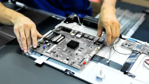
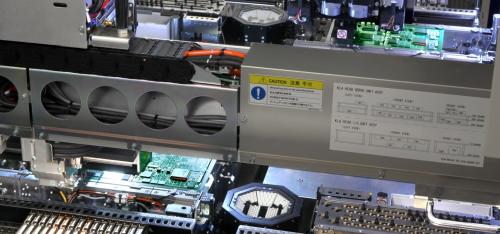
Box Build

Box Build
Box build in electronics refers to the process of assembling and integrating electronic components into a complete product enclosure. It involves mechanical assembly, wiring, testing and packaging to create a fully functional device. Some key aspects of box build assembly include:
PCB Integration: installing printed circuit boards into enclosures
Cable & Wiring Harness Assembly: connecting internal components for power and signal transmission
Mechanical Assembly: fitting enclosures, brackets and fasteners
Firmware & Software Loading: programming devices before final testing
Functional Testing & Quality Assurance: ensuring the product meets performance standards
Packaging & Labelling: preparing the final product for distribution
Conformal Coating

Conformal Coating
Conformal coating is a protective layer applied to printed circuit boards (PCBs) to shield them from environmental factors like moisture, dust, chemicals and temperature extremes. It helps improve the reliability and longevity of electronic components, especially in harsh conditions. There are different types of conformal coating including:
Acrylic (AR) – easy to apply and remove, offering good moisture resistance
Silicone (SR) – excellent flexibility and protection against high temperatures
Polyurethane (UR) – strong chemical resistance and durability
Epoxy (ER) – tough and resistant to abrasion but harder to remove
Parylene (XY) – provides superior protection with a uniform, ultra-thin coating
Typical application methods include:
Brushing – simple but prone to uneven coverage
Spraying – common for mass production, ensuring consistent coating
Dipping – effective for full coverage but may require masking
Selective Coating – applied by robots for precision
TechPoint specialises in harsh environment electronics, including conformal coating, potting and encapsulation for aerospace, automotive, marine, military and industrial applications.

Full Turnkey Solutions

Full Turnkey Solutions
Our turnkey solutions refer to end-to-end manufacturing services, where TechPoint handles everything from design and prototyping to assembly, testing and final product delivery. This approach simplifies the supply chain, reduces costs and ensures consistency in quality. Key Features include:
Component Sourcing – Procurement of high-quality electronic components
PCB Assembly – SMT and THT assembly for reliable circuit boards
Testing & Quality Control – Functional testing, AOI and environmental stress testing
Final Product Assembly – Enclosure integration, cable harnessing and system validation
Logistics & Distribution – Packaging, barcoding and direct shipment to customers
Benefits of our full turnkey solutions
Cost Efficiency – reduces overheads by consolidating processes
Faster Time-to-Market – streamlined production accelerates delivery
Quality Assurance – consistent standards across all stages
Supply Chain Simplification – eliminates the need for multiple vendors
TechPoint specialises in full turnkey electronics manufacturing, offering design, assembly, testing and supply chain solutions for industries like aerospace, automotive, marine, military and industrial automation.
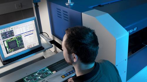
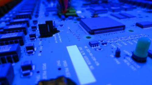
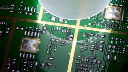
Printed Circuit Board Assembly (PCBA)

Printed Circuit Board Assembly (PCBA)
PCBA is the process of soldering electronic components onto a Printed Circuit Board (PCB) to create a functional electronic device. It involves several key steps:
PCB Fabrication: manufacturing the bare board with copper traces
Component Placement: using automated pick-and-place machines to position components
Soldering: applying solder paste and using reflow or wave soldering to secure components
Inspection & Testing: conducting Automated Optical Inspection (AOI), X-ray testing and functional tests to ensure quality
Final Assembly: integrating the PCB into enclosures or larger systems
Printed Circuit Board Assembly (PCBA) Inspection

Printed Circuit Board Assembly (PCBA) Inspection
PCBA inspection is a crucial step in electronics manufacturing to ensure quality and reliability. It involves various methods to detect defects and verify that the assembly meets industry standards. Common inspection techniques that we use include:
Visual Inspection – a manual check for physical defects like misaligned components, poor solder joints or damage
Automated Optical Inspection (AOI) – uses cameras and software to detect missing components, misalignment and soldering defects
X-Ray Inspection (AXI) – helps identify hidden defects in multilayer PCBs, especially for components like Ball Grid Arrays (BGAs)
In-Circuit Testing (ICT) – checks electrical connections and verifies component functionality
Functional Testing – ensures the assembled PCB performs as intended in real-world applications
Solderability Testing – confirms the durability and reliability of the solder joints
Printed Circuit Board Assembly (PCBA) Production

Printed Circuit Board Assembly (PCBA) Production
PCBA (Printed Circuit Board Assembly) production is a key process in electronics manufacturing, where electronic components are mounted onto a PCB to create a functional device. The process typically involves:
Design & Fabrication – creating schematics and manufacturing the PCB
Component Placement – mounting electronic components onto the board
Soldering – using techniques like SMT (Surface Mount Technology) or THT (Through-Hole Technology) to secure components
Inspection & Testing – ensuring quality through automated optical inspection (AOI), functional testing and X-ray analysis
Final Assembly & Packaging – completing the product for shipment
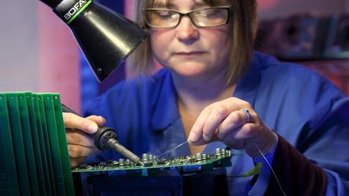
Printed Circuit Board Assembly (PCBA) Rework & Repairs

Printed Circuit Board Assembly (PCBA) Rework & Repairs
PCBA rework and repairs are essential processes in electronics manufacturing, allowing manufacturers to fix defects, replace faulty components and restore functionality without discarding entire assemblies. These techniques help improve product reliability, reduce costs and minimise waste. Common PCBA rework & repair techniques that we carry out include:
Component Replacement – removing and replacing defective or outdated components
Soldering Rework – fixing soldering defects like cold joints, bridging or insufficient solder
BGA Rework – specialised techniques for reballing and replacing Ball Grid Array (BGA) components
Trace Repair – restoring damaged PCB traces to maintain electrical connectivity
Conformal Coating Removal & Reapplication – repairing protective coatings for environmental resistance
Failure Analysis & Debugging – identifying root causes of defects and implementing corrective actions
Printed Circuit Board Assembly (PCBA) Testing & Analysis

Printed Circuit Board Assembly (PCBA) Testing & Analysis
PCBA testing and analysis are crucial steps in electronics manufacturing to ensure reliability, functionality and compliance with industry standards. These processes help detect defects, verify performance and improve product quality. Common PCBA testing methods include:
Visual Inspection – manual or automated checks for soldering defects, misaligned components and physical damage
Automated Optical Inspection (AOI) – uses cameras and software to detect missing components, misalignment and soldering issues
X-Ray Inspection (AXI) – identifies hidden defects in multilayer PCBs, especially for components like Ball Grid Arrays (BGAs)
In-Circuit Testing (ICT) – verifies electrical connections and component functionality
Functional Testing – ensures the assembled PCB performs as intended in real-world applications
Environmental Stress Testing – simulates extreme conditions like temperature, humidity and vibration to assess durability
Failure Analysis – investigates defects using techniques like thermal cycling, mechanical stress tests and electrical load testing
PCBA testing provides the following benefits:
Improves reliability – detects faults early to prevent failures in the field
Reduces costs – identifies defects before mass production, minimising rework and recalls
Ensures compliance – meets industry standards for safety and performance
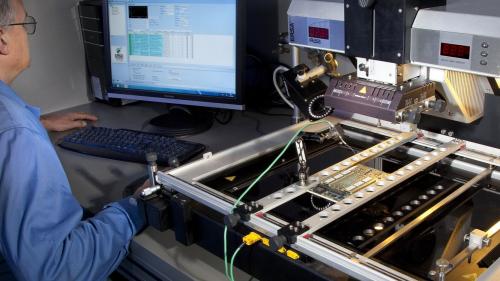
Robotic Through-Hole (TH) Soldering

Robotic Through-Hole (TH) Soldering
This is an advanced automation technique used in electronics manufacturing to improve precision, efficiency and consistency in soldering through-hole components onto printed circuit boards (PCBs). Unlike manual soldering, robotic systems ensure repeatability and reduce human error. Key features of our robotic TH soldering include:
Automated Precision – robots apply solder with exact temperature and placement, minimising defects
Consistency & Speed – faster than manual soldering, ensuring uniform joints across production batches
Reduced Labor Costs – minimises reliance on skilled manual soldering operators
Improved Quality Control – integrated inspection systems detect defects in real time
Adaptability – supports various soldering techniques including iron tip, laser and ultrasonic soldering
Common applications for TH soldering are:
Automotive Electronics – reliable soldering for vehicle control systems
Aerospace & Defence – high-precision soldering for mission-critical electronics
Medical Devices – ensuring durability and compliance with strict regulations
Industrial Automation – robust soldering for factory automation systems
Second Stage Processing

Second Stage Processing
Second-stage processing in electronics refers to the additional steps taken after the initial assembly phase to refine, enhance, or finalise a product. This stage is crucial for ensuring reliability, functionality and compliance with industry standards. Common second-stage processes include:
Through-Hole Soldering – adding components that require manual or automated soldering
Press-Fit Technology – using solder-free connectors for reliable electrical connections
Rework & Repairs – fixing defects or replacing components to ensure functionality
Conformal Coating & Encapsulation – protecting PCBs from environmental factors
Final Assembly & Testing – ensuring the product meets quality standards before shipment
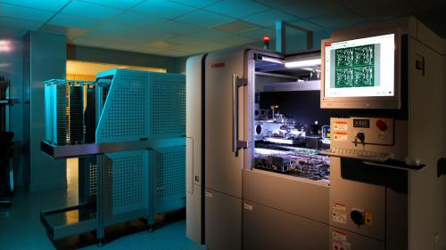
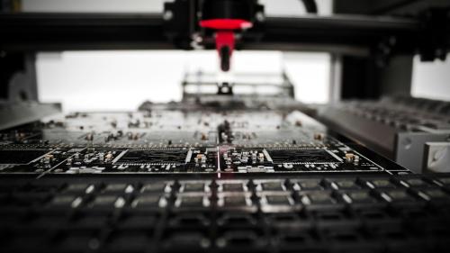
SMT Services

SMT Services
Our SMT services enable the efficient assembly of components onto printed circuit boards (PCBs). SMT offers higher precision, automation and miniaturisation, making it ideal for modern electronic devices. These include:
PCB Assembly – automated placement of surface mount components
Solder Paste Printing – precise application of solder paste for component attachment
Pick-and-Place Assembly – high-speed robotic placement of components
Reflow Soldering – controlled heating to secure components
Automated Optical Inspection (AOI) – detecting defects and ensuring quality
X-Ray Inspection (AXI) – identifying hidden soldering issues in complex assemblies
Functional Testing – verifying electrical performance and reliability
Solder Jet Printing

Solder Jet Printing
This is an advanced technique used in electronics manufacturing to apply solder paste directly onto PCB pads without the need for traditional stencil tooling. This method offers greater precision, flexibility and efficiency making it ideal for complex assemblies. Key benefits include:
Eliminates Stencil Tooling – no need for costly and time-consuming stencil fabrication
Precise Paste Deposition – allows for controlled solder paste application, reducing defects
Faster Turnaround – can start within minutes of receiving bare boards
Adaptability – works with irregular component outlines, thermal pads and paste-free zones
Improved Yield – reduces common soldering issues like floating Quad Flat No-leads (QFN) devices and excessive solder
Typical applications for solder jet printing are:
RF Assemblies – enhances reliability in high-frequency circuits
Micro-Packaging – enables precise solder paste deposition on substrates beyond PCBs
Advanced PCB Designs – supports HDI, Package-on-Package (PoP), Quad Flat No-leads (QFN) and cavity printing
Testing Solutions & Radio Frequency (RF) Engineering

Testing Solutions & Radio Frequency (RF) Engineering
Testing and RF engineering are essential in electronics manufacturing, ensuring signal integrity, performance and compliance with industry standards. These processes help optimise wireless communication, reduce interference and improve product reliability. Typical testing solutions that we provide include:
Automated Optical Inspection (AOI) – detects defects in PCB assemblies
X-Ray Inspection (AXI) – identifies hidden soldering issues in complex components
In-Circuit Testing (ICT) – verifies electrical connections and component functionality
Functional Testing – ensures the assembled PCB performs as intended
Environmental Stress Testing – simulates extreme conditions like temperature and vibration
TechPoint’s in-house RF engineering & testing laboratory services include:
RF Signal Integrity Testing – evaluating transmission quality and interference
Antenna Performance Analysis – optimising wireless communication efficiency
Electromagnetic Compatibility (EMC) Testing – ensuring compliance with regulatory standards
RF Shielding & Isolation – reducing unwanted signal interference
Wireless Protocol Testing – validating Bluetooth, Wi-Fi and cellular communication
Vapour Phase, Nitrogen & Conventional Reflow Process

Vapour Phase, Nitrogen & Conventional Reflow Process
Reflow soldering is a critical process in electronics manufacturing, used to attach surface mount components to printed circuit boards (PCBs). We use three main types of reflow processes: vapour phase, nitrogen and conventional convection reflow, each with unique advantages:
Vapour Phase Reflow
Uses a heat transfer liquid (e.g., Galden) that vaporises to create a controlled heating environment
Provides uniform heating across the PCB, reducing thermal stress
Minimises void formation in solder joints, improving reliability
Ideal for high-density assemblies and complex components
Nitrogen Reflow
Uses nitrogen gas to create an inert atmosphere, preventing oxidation
Improves solder joint integrity, especially for lead-free soldering
Reduces defects like solder balling and bridging
Commonly used in automotive, aerospace and medical electronics
Conventional Convection Reflow
The most widely used method, relying on heated air circulation
Involves preheat, soak, reflow and cooling phases
Works well for standard PCB assemblies with consistent thermal profiles
Cost-effective and compatible with high-volume production